
Chemical Etching Services: The Buyer's Guide to Precision Metal Parts
Selecting the right manufacturing process is one of the most important decisions engineers make during product development. The process influences everything from component performance and manufacturability to cost, lead time, and production scalability. For thin metal components requiring intricate features, tight tolerances, and repeatable quality, traditional manufacturing methods are not always the best solution.
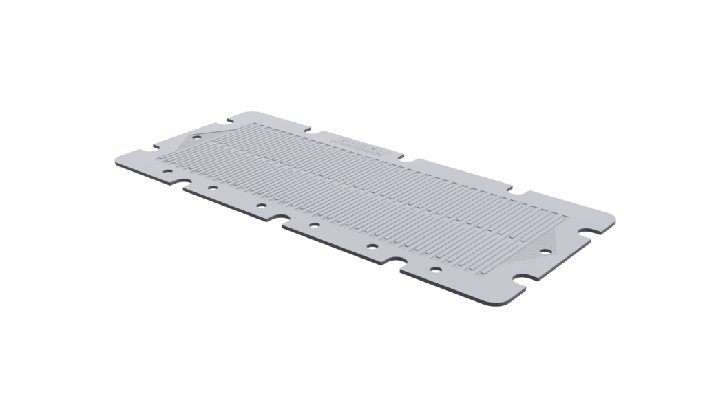
Chemical etching, on the other hand, enables engineers to manufacture highly accurate precision components without introducing mechanical stress, burrs, or heat-affected zones. Offering exceptional design freedom while eliminating many of the tooling costs associated with stamping and other hard-tooling methods, it's easy to see why chemical etching has quickly become the preferred manufacturing method.
Today, chemical etching is used to create lightweight, intricate metal parts in aerospace and automotive industries, and beyond! Its precision-etched components can be found in everything from electronics and medical devices to RF and microwave systems, energy infrastructure, and industrial automation.
Fotofab has spent decades helping engineers determine whether the chemical etching process is the right manufacturing solution for their applications. From initial design guidance and material selection through production and manufacturing, our team supports customers developing precision metal parts for some of the world's most demanding industries.
This page explains everything engineers should know before specifying chemically etched components, including how the process works, where it excels, how it compares to other manufacturing processes, and the key design considerations that influence manufacturability.
What Is Chemical Etching?
Understanding the Chemical Etching Process
Also known as photo chemical etching, photo etching, chemical milling, or metal etching, chemical etching is a subtractive manufacturing method that removes carefully controlled amounts of metal from a sheet using chemistry rather than mechanical cutting.
Unlike machining, stamping, or laser cutting, no cutting tools ever contact the workpiece. Instead, selected areas of the material are protected while the exposed metal is dissolved by a precisely controlled chemical etchant.
The result is an accurate metal component with exceptional detail, smooth edges, and outstanding repeatability.
Because the process removes material uniformly from both sides of the workpiece, engineers can produce intricate designs that would be difficult—or impossible—to manufacture using conventional fabrication techniques.
The process is especially effective for thin materials in which preserving flatness, dimensional stability, and the original metal properties is essential.
Engineers increasingly specify photochemical etching because it enables rapid design changes, supports complex geometries, and delivers cost-effective production from prototype quantities through high-volume production.
Learn more: Download our Photochemical Machining (PCM) Whitepaper
What Makes Chemical Etching “Precision”?
Precision Etching Defined
The difference between basic etching and precision etching lies in process control, repeatability, and engineering oversight. Mechanical methods depend on tooling accuracy and tool condition. Precision chemical etching depends on controlled chemistry, calibrated exposure systems, and tightly managed process parameters.
Process Control vs Mechanical Accuracy
In mechanical cutting, tool wear directly impacts dimensional consistency. In precision chemical etching, there is no tool wear. Feature accuracy is governed by photoresist imaging and chemistry control, enabling predictable outcomes even across complex layouts.
Role of Photoresist Imaging
The photochemical imaging stage determines the final part geometry. High-resolution digital blueprints or artwork transfers patterns directly to the metal surface, allowing intricate designs, dense feature arrays, and fine geometries to be reproduced with exceptional fidelity.
Repeatability and Feature Density
Because etching removes material uniformly, it supports high feature density and tight spacing without distortion. This makes it particularly effective for detailed components where precision and consistency are critical.
How Photo Chemical Etching Works
Although individual manufacturers may use proprietary equipment or chemistry, the fundamental workflow remains similar.
Step 1: Material Selection
Every project begins by selecting the most appropriate engineering material.
Factors influencing material compatibility include:
- Mechanical strength
- Corrosion resistance
- Electrical conductivity
- Thermal performance
- Magnetic characteristics
- Required metal thickness
- Operating environment
Fotofab offers etching and fabrication services for a wide range of metals, including pure metals and alloys that are difficult to machine. We have full and half-hard materials as well as annealed materials available. Below is a list of standard metals we etch. Etching thicknesses range from 0.010 mm to 2.5 mm.
Choosing the correct material early helps optimize both manufacturability and final component performance.
Need help choosing a metal? See our Photochemical Etching Materials Reference Guide to compare material properties, applications, and etching considerations.
Step 2: Material Preparation
Before imaging begins, the metal sheets are carefully prepared.
Each sheet is chemically cleaned to remove oils, oxidation, fingerprints, and contaminants from the metal surface. This preparation ensures proper adhesion of the photoresist while improving imaging consistency across the entire panel.
Clean preparation is a critical step because contamination can affect image quality and ultimately influence the final etched components.
Step 3: Photoresist Imaging
A light-sensitive photoresist is laminated onto both sides of the required sheet metal.
Digital artwork representing the final design is transferred onto the resist using precision imaging equipment. During exposure, UV light hardens only the desired image while protecting areas that will remain after etching.
Once developed, the photoresist forms a permanent etched image that acts as a protective mask during the etching operation.
Step 4: Chemical Etching
The protected sheet enters an automated etching machine where both sides are sprayed with a carefully controlled etching solution.
Depending on the material being processed, different chemistries may be used. For example, ferric chloride is commonly used when etching copper and many stainless steel applications, while other alloys require specialized chemistry.
As the corrosive chemical dissolves the exposed metal, the protected regions remain intact.
Because no mechanical force is applied, the process preserves the material's original grain structure while producing highly accurate features with exceptional edge quality.
Step 5: Finishing
Once the desired geometry has been achieved, the remaining photoresist is removed.
The finished components produced are then cleaned, inspected, and prepared for any required secondary operations such as:
- Forming
- Plating
- Diffusion bonding
- Electropolishing
- Heat treatment
- Laser engraving
- Assembly
The result is a stress-free precision component ready for prototype evaluation or production assembly.
Chemical Etching Compared with Other Manufacturing Processes
Every manufacturing process has strengths and limitations. Understanding these differences helps engineers select the best technology for each application.
Chemical Etching vs Laser Cutting
Laser cutting is widely used for thicker materials and structural components.
However, localized heating can create heat-affected zones, microstructural changes, and slight distortion—particularly in thin metals.
Photochemical etching avoids these issues entirely because material removal occurs chemically rather than thermally.
Additional advantages include:
- Superior feature quality
- Better edge consistency
- No burr formation
- No thermal distortion
- Greater precision on thin materials
For highly detailed precision components, photochemical etching generally produces more consistent results.
Chemical Etching vs Stamping
Stamping remains one of the most economical options for very high production volumes.
Its primary limitation is tooling.
Progressive dies often require significant investment before production begins, making stamping less attractive for prototypes or evolving designs.
Photo etching eliminates expensive tooling costs by replacing dies with digital artwork.
This allows engineers to:
- Modify designs rapidly
- Evaluate multiple design concepts
- Reduce upfront investment
- Accelerate prototype delivery
Projects involving frequent revisions often benefit significantly from this flexibility.
Chemical Etching vs Machining
Traditional machining offers excellent three-dimensional capability but becomes increasingly expensive as features become smaller and more complex.
Fine slots, perforations, internal geometries, and thin walls frequently require multiple machining operations.
Chemical etching excels at producing these complex geometries in a single manufacturing operation while generating significantly less material waste.
Because complexity has relatively little impact on manufacturing cost, engineers are free to optimize performance rather than simplify designs for manufacturing.
Chemical Etching vs EDM
Electrical discharge machining provides outstanding accuracy for certain applications but is generally slower than photochemical etching and less economical for larger production quantities.
EDM is often selected for thick materials or specialized tooling.
Photochemical etching typically offers advantages in:
- Throughput
- Prototype turnaround
- Production scalability
- Lower cost for thin metal components
- Simultaneous manufacture of multiple components on a single sheet
For many precision sheet metal applications, photo chemical etching delivers an excellent balance of speed, accuracy, and manufacturing efficiency.
The Main Benefits of Chemical Etching
Choosing the right manufacturing process isn't simply about producing a part. It's about balancing precision, cost, lead time, material performance, and production scalability. Photochemical etching offers a unique combination of advantages that make it one of the most versatile manufacturing methods for thin metal components.
Precision Without Burrs
One of the biggest advantages of photochemical etching is its ability to produce highly accurate parts without introducing burrs or deformation typically associated with punching, stamping, or mechanical cutting.
Because the material is dissolved rather than cut, edges remain clean and consistent, often eliminating secondary deburring operations. This is especially important for components used in medical devices, optical systems, precision electronics, and semiconductor equipment where edge quality directly affects performance.
No Heat-Affected Zones
Unlike laser cutting or other thermal manufacturing processes, photochemical etching introduces no heat into the workpiece.
This preserves the material's original mechanical properties while eliminating distortion, residual stresses, and metallurgical changes that can occur during heat-based fabrication.
Maintaining the original grain structure is particularly valuable when working with thin materials or specialty alloys where dimensional stability is critical.
Complex Geometries
As products become smaller and more sophisticated, component complexity continues to increase.
Photochemical etching allows engineers to manufacture:
- Fine slots
- Intricate openings
- Precision perforations
- Internal cut-outs
- Complex lattice structures
- Detailed mesh patterns
- Decorative features
- Identification markings
Unlike many conventional manufacturing methods, increasing geometric complexity has little impact on tooling or production costs.
This gives engineers far greater freedom during product development.
Rapid Design Changes
Product development rarely follows a straight path.
Design revisions, testing feedback, and performance improvements often require multiple iterations before a component is finalized.
Because photochemical etching uses digital artwork rather than hard tooling, design modifications can be implemented quickly without the expense of manufacturing new dies or fixtures.
This flexibility significantly shortens development cycles while allowing engineers to evaluate multiple design concepts with confidence.
Tooling-Free Prototyping
Traditional manufacturing methods frequently require substantial upfront investment before a single part is produced.
Photochemical etching removes this barrier.
Without expensive tooling, engineers can produce prototype quantities quickly and economically, making the process ideal for early-stage development, proof-of-concept work, and design validation.
Production Scalability
While photochemical etching is well known for rapid prototyping, it also scales efficiently into production.
Whether manufacturing a handful of prototypes or thousands of production parts, the same digital workflow supports consistent quality and repeatability without tooling wear affecting dimensional accuracy.
Material Versatility
Few precision manufacturing methods support as many engineering materials as photochemical etching.
This flexibility allows engineers to optimize performance based on application requirements rather than manufacturing limitations.
What Sets Chemical Etching Apart?
Precision etching is not simply a chemistry exercise; it is a disciplined manufacturing process requiring technical expertise and rigorous quality control.
Engineering Collaboration and DFM
Fotofab works closely with engineers to optimize designs for manufacturability. Early-stage collaboration ensures appropriate material selection, layout optimization, and predictable etch factor compensation before production begins.
Controlled Chemistry and Process Parameters
Our facilities maintain strict control over temperature, chemistry concentration, dwell time, and agitation. Every variable is monitored to ensure dimensional accuracy and surface integrity.
Inspection and Quality Systems
We integrate in-process inspection and final verification to ensure compliance with customer specifications. Quality systems are structured to support repeatability across low-volume prototypes and full-scale production.
Single- and Double-Sided Etching
Fotofab supports both single-sided and double-sided photo chemical etching configurations, enabling through-features, partial etches, and stepped geometries within a single manufacturing process.
Prototype Through Production
Because the process requires minimal hard tooling, customers benefit from rapid iteration and scalability. Whether producing small runs of custom metal parts or high-volume precision components, Fotofab maintains consistent output.
Learn more: Download our Photochemical Machining (PCM) Whitepaper
Materials for Chemical Etching
Material selection influences everything from mechanical performance and corrosion resistance to electrical conductivity, manufacturability, and overall product life.
Did you know that over 2000 different metal types can be etched using this process?
Fotofab works with an extensive range of engineering materials to support applications across aerospace, defense, electronics, medical, industrial, RF, semiconductor, and energy markets.
Stainless Steel
Stainless steel remains one of the most commonly specified materials for precision-etched components due to its excellent balance of corrosion resistance, strength, and cost.
Typical applications include:
- Precision shims
- Medical instruments
- Springs
- Filters
- Precision screens
- Electronic assemblies
Fotofab specializes in the chemical etching of stainless steel alloys, including the 301, 302/304, 316/316L, and 400 series, catering to a broad spectrum of applications and industries.
Learn more about our Stainless Steel capabilities.
Titanium
Titanium combines exceptional strength with low weight and outstanding corrosion resistance.
It is frequently specified for:
- Aerospace components
- Medical implants
- Chemical processing equipment
- High-performance thermal systems
Fotofab routinely manufactures parts quickly and safely from Titanium in a wide range of alloys. When using photo etching, there is no added cost to add a feature, whether you need a thousand holes in a part or a single hole.
Explore our Titanium Etching.
Aluminum
Aluminum offers lightweight performance, good conductivity, and excellent machinability.
It is commonly used for:
- Lightweight structural components
- Heat management products
- Electronics
- Aerospace assemblies
At Fotofab, we apply advanced photochemical etching techniques to deliver precise, stress-free aluminum components with no mechanical burrs that perform reliably in even the most demanding environments.
Learn more about our Aluminum Etching process.
Copper and Copper Alloys
Copper provides excellent electrical and thermal conductivity.
Applications include:
- Electrical contacts
- RF shielding
- Heat transfer components
- Precision connectors
- Thermal management systems
Fotofab is a leader in the precision chemical etching of copper, offering components across a diverse range of industries. Our expertise extends from the etching of delicate copper foils for printed circuit boards to the creation of robust, corrosion-resistant parts suitable for harsh environments.
Explore our Copper etching expertise.
Brass
Brass combines corrosion resistance with attractive cosmetic appearance and excellent electrical performance.
It is commonly selected for decorative and electrical applications requiring precision manufacturing.
At Fotofab, we specialize in the precision chemical etching of brass, crafting components that meet your exact specifications. Our advanced photochemical etching process allows for exceptional detail and accuracy, ideal for both delicate and robust applications.
Learn more about our Brass etching process.
Kovar
Kovar is widely used where controlled thermal expansion is essential.
Typical applications include:
- Hermetic packages
- Electronic housings
- Aerospace electronics
- Semiconductor assemblies
Fotofab’s etching process produces designs that can withstand harsh indoor and outdoor environments. The process uses an acid (Ferric Chloride) to etch into unprotected parts of a metal surface to create a design or image formed to your project’s specifications.
View our Kovar capabilities.
Molybdenum
Molybdenum performs exceptionally well in high-temperature and vacuum environments.
Applications include:
- Semiconductor equipment
- Heat shields
- Precision apertures
- Furnace components
Our acid etching of Molybdenum delivers components that perform exceptionally in extreme-heat environments.
Learn about our Molybdenum Etching.
Inconel
Inconel provides exceptional strength and oxidation resistance under extreme temperatures.
Common applications include:
- Aerospace
- Gas turbines
- Energy systems
- Chemical processing
Fotofab is a leader in precision etching for Inconel alloys. Offering high-quality components for demanding industries since 1967, our expertise ranges from etching delicate Inconel foils for precise circuit applications to creating corrosion-resistant parts designed for the most challenging environments.
View our Inconel capabilities.
Beryllium Copper
Beryllium copper combines high strength with excellent conductivity and fatigue resistance.
Typical applications include:
- Electrical contacts
- Springs
- Aerospace electronics
- Defense systems
Our Beryllium Copper chemical etching is ideal for applications in electrical and electronic industries, such as contact and spring contact applications.
Learn about our Beryllium Copper Etching.
Phosphor Bronze
Phosphor bronze offers excellent wear resistance, fatigue life, and electrical conductivity.
It is frequently used for:
- Springs
- Contacts
- Precision electrical components
Fotofab’s chemical etching process produces designs that can withstand harsh indoor and outdoor environments. The process uses an acid (Ferric Chloride) to etch into unprotected parts of a metal surface to create a design or image formed to your project’s specifications.
View our Phosphor Bronze capabilities.
Mu Metal
Mu Metal is a high-permeability alloy designed for magnetic shielding applications.
Engineers commonly specify it for:
- EMI shielding
- RF shielding
- Scientific instruments
- Sensitive electronic equipment
Learn about our Mu Metal Etching.
Explore our complete Materials Hub to compare engineering materials and determine the best option for your application.
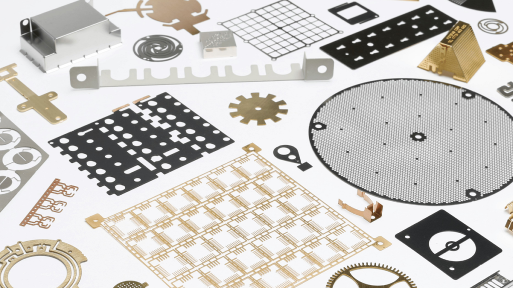
Design Considerations for Precision Etched Parts
Understanding the design principles behind photochemical etching helps engineers maximize performance while minimizing manufacturing costs.
Feature Size and Tight Tolerances
Photochemical etching is capable of producing remarkably fine features with excellent repeatability.
Minimum feature sizes depend primarily on material thickness, alloy selection, and overall part geometry rather than tooling limitations.
Working with Fotofab early in the design process allows engineers to optimize dimensions for both manufacturability and performance.
Material Thickness
The thickness of the starting material directly influences achievable feature sizes, hole diameters, slot widths, and overall dimensional capability.
Generally, thinner materials enable finer detail, while thicker materials support greater structural performance.
Selecting the appropriate thickness requires balancing functional requirements with manufacturing capability.
Understanding Etch Factor
One of the most important concepts in photochemical etching is the etch factor.
Because material is removed from both sides simultaneously, etched features naturally develop a slight sidewall taper.
Experienced engineers account for this characteristic during the design phase to ensure finished components meet dimensional requirements.
Fotofab's engineering team routinely assists customers in optimizing designs around etch characteristics without compromising functionality.
Part Geometry
Photochemical etching excels at producing intricate flat components with highly detailed internal features.
Examples include:
- Fine meshes
- Optical encoder discs
- Apertures
- Flow fields
- Filters
- Shielding structures
- Precision springs
- Decorative panels
Since complexity has relatively little effect on manufacturing cost, engineers are free to prioritize performance over manufacturing convenience.
Benefits of Burr-Free Design
Clean edge quality contributes to:
- Improved assembly
- Better mating surfaces
- Reduced contamination
- Lower friction
- Improved electrical performance
- Enhanced cosmetic appearance
In many applications, eliminating burrs reduces secondary finishing requirements while improving overall product quality.
Primary Cost Drivers
Unlike stamping or machining, complexity is rarely the primary cost driver in photochemical etching.
Instead, project costs are typically influenced by:
- Material selection
- Material thickness
- Overall sheet utilization
- Quantity
- Secondary operations
- Inspection requirements
Understanding these variables early allows engineers to optimize both cost and manufacturability.
Design for Manufacturability
Successful projects begin with collaboration.
By involving Fotofab's engineering team during the design phase, customers can:
- Improve manufacturability
- Reduce material waste
- Simplify production
- Optimize tolerances
- Shorten development schedules
- Lower overall production costs
Early engineering collaboration often produces better-performing components while reducing total project risk.
Key Applications of Chemical Etching
Precision Metal Etching Across Modern Manufacturing Industries
Precision chemical etching supports a wide range of industries and applications where tight tolerances, fine detail, and burr-free edges are essential. Below is how chemically etched parts are applied across key sectors.
Aerospace & Defense
Aerospace and defense applications demand lightweight, reliable components capable of performing in harsh operating environments.
Fotofab manufactures precision-etched components used in:
- RF and microwave systems
- Thermal management assemblies
- Optical encoder discs
- Sensor components
- EMI/RFI shielding
- Precision brackets and structural components
- Aerospace instrumentation
As a premier full-service supplier, Fotofab helps aerospace engineers move quickly from prototype to production without sacrificing quality. With low-cost digital tooling, design iterations can be made rapidly, accelerating innovation while reducing lead times.
Fotofab’s components are known for being lightweight, durable, and reliable, supporting both civilian and military flight systems where every gram matters. Our subtractive manufacturing process enables the creation of complex geometries that would be costly or impossible to achieve through CNC machining or laser cutting.
Learn more about our Aerospace and Defense capabilities.
Energy Systems
Modern energy systems require precision metal components capable of performing in demanding thermal and mechanical environments.
Applications include:
- Fuel cell components
- Thermal management systems
- Precision separators
- Power generation equipment
- Hydrogen technologies
- Energy storage assemblies
These industries demonstrate the remarkable flexibility of photochemical etching across virtually every advanced manufacturing sector.
Fotofab photochemically etches a range of precision metal parts for the energy industry, which includes all involved in the production and sale of energy, like fuel extraction, manufacturing, refining, and distribution. We also service the many markets that fall under the Energy umbrella.
View our Energy page.
Semiconductor Equipment
Semiconductor manufacturing depends on extremely accurate thin-metal components capable of operating in demanding cleanroom environments.
Typical applications include:
- Precision apertures
- Wafer processing components
- Vacuum system hardware
- Thermal management plates
- Alignment features
- Precision masks
Learn more about our Semiconductor solutions.
Medical Devices
Medical manufacturers require miniature components with exceptional dimensional accuracy, clean edges, and consistent repeatability.
Photochemical etching supports:
- Surgical instruments
- Implantable device components
- Diagnostic equipment
- Medical filters and screens
- Precision sensing components
- Micro-scale assemblies
Fotofab specializes in photochemical etching of medical-grade materials, which is a precise process that allows for extremely tight tolerances and configurations not possible with traditional metal fabrication methods.
Explore our Medical market expertise.
Electronics & RF Systems
As electronic assemblies continue to shrink, component precision becomes increasingly important.
Photochemical etching enables:
- EMI/RFI shielding
- Electrical contacts
- RF components
- Connectors
- Lead frames
- Precision springs
- Heat transfer components
Fotofab photochemically etches a variety of custom and standard metal parts and components for the electronics marketplace.
View our Electronics and RF & Microwave pages.
Industrial Systems
Industrial equipment often requires durable precision components capable of operating continuously under demanding conditions.
Examples include:
- Precision filters
- Flow control components
- Mechanical assemblies
- Instrumentation hardware
- Wear-resistant components
- Fluid control devices
At Fotofab, providing clients with quality products is our utmost priority. We purchase from reputable suppliers across the US, verify compliance upon arrival, confirm accuracy with precision testing, and audit completed orders prior to shipment.
Learn more about our Industrial solutions.
Common Precision Etched Components
Metal Etching Products Engineers Specify Every Day
Many engineers interact with etched components without realizing how they are manufactured.
Some of Fotofab's most common products include:
Optical Encoder Discs
Encoder discs require extremely accurate slot spacing and feature geometry to ensure reliable motion feedback.
Chemical etching of metal delivers the precision necessary for high-resolution optical encoding systems.
Learn more about Optical Encoder Discs.
Precision Shims
Precision shims provide accurate spacing and alignment throughout aerospace, electronics, semiconductor, and medical assemblies.
Because photochemical etching maintains consistent thickness while producing complex profiles, it is ideal for custom shim manufacturing.
Explore Precision Shims.
EMI/RFI Shielding
Modern electronic systems require effective electromagnetic shielding to maintain signal integrity and reduce interference.
Fotofab manufactures precision shielding enclosures featuring:
- Intricate ventilation patterns
- Foldable bend channels
- Complex internal walls
- High dimensional accuracy
Learn more about EMI/RFI Shielding.
Filters and Screens
Precision filters and screens support applications involving:
- Fluid control
- Particle separation
- Chemical processing
- Medical filtration
- Semiconductor manufacturing
- Analytical instrumentation
Complex mesh geometries can be produced economically without expensive tooling.
Precision Apertures
Apertures control light, particle flow, radiation, or fluid movement in numerous scientific and industrial systems.
Etching enables extremely accurate openings while preserving delicate material properties.
Medical Components
Medical devices frequently utilize etched:
- Surgical blades
- Implant components
- Diagnostic assemblies
- Sensor elements
- Precision meshes
Springs and Contacts
Thin etched springs and electrical contacts provide consistent mechanical performance while allowing highly customized geometries.
Applications include connectors, switches, sensing devices, and miniature electronic assemblies.
Learn more about our precision springs and contacts.
Semiconductor Components
Photochemical etching supports precision semiconductor hardware, including:
- Process apertures
- Alignment components
- Precision masks
- Thermal management plates
- Vacuum hardware
Discover our range of semiconductor components.
In need of custom components? We do that too!
Explore our complete Products library to discover additional component types.
Why Engineers Choose Fotofab
Choosing a manufacturing partner involves more than comparing capabilities. Engineers need confidence that their supplier understands design intent, material behavior, manufacturing constraints, and long-term production requirements.
For decades, Fotofab has worked alongside engineers to develop precision components that perform reliably in demanding applications. Here's what sets us apart:
Broad Material Expertise
Our team supports one of the industry's broadest selections of precision etching materials, allowing engineers to optimize component performance without compromising manufacturability.
Rapid Prototyping
Because photochemical etching eliminates hard tooling, prototype parts can be produced quickly, allowing engineering teams to validate designs, evaluate alternatives, and accelerate product development.
Production Scalability
Whether producing a handful of prototypes or full production quantities, Fotofab delivers consistent quality and repeatable manufacturing processes.
Precision Manufacturing Experience
Every project benefits from decades of engineering knowledge in precision photochemical etching, design optimization, secondary operations, and quality assurance.
Multi-Industry Expertise
Our experience spans many of the world's most demanding industries, including:
- Aerospace
- Defense
- Medical
- Semiconductor
- Electronics
- RF & Microwave
- Energy
- Industrial Automation
This broad industry knowledge allows us to recommend practical manufacturing solutions based on real-world engineering experience rather than theoretical capability.
View all the sectors we serve.
Fotofab Resources
One advantage of working with Fotofab is access to a complete ecosystem of engineering resources designed to help you make informed manufacturing decisions.
Fotofab uses the photochemical machining process to produce a wide variety of precision parts from thin metal sheets. Not many are familiar with the process, so our “Design Guide to Photochemical Machining” was created specifically for those who are involved with the designing and/or purchasing of metal parts.
Photochemical Machining Design Resources
The Design Guide provides you with:
- Engineering advantages of photochemical machining.
- Overview of our photochemical machining process.
- Considerations for the design of your thin metal parts.
- Considerations for your engineering drawings/sketches.
Fotofab offers free consultation and quotation for your specific designs and is available to assist you with your metal parts requirements. By designing with an awareness of our process capabilities, you will minimize the cost and delivery time of your metal parts, whether for prototyping or production.
Explore our additional resources:
Start Your Next Precision Etching Project
Every successful precision component begins with selecting the right manufacturing process.
Photochemical etching offers a unique combination of precision, flexibility, speed, and manufacturability that few other technologies can match. By eliminating mechanical stress, tooling constraints, and heat distortion, engineers can produce complex metal components that meet demanding performance requirements while accelerating development and controlling costs.
Whether you're evaluating manufacturing options, selecting materials, designing a new component, or preparing for production, Fotofab's engineering team is ready to help.
Our collaborative approach, broad material expertise, and decades of photochemical etching experience enable us to support projects ranging from early-stage prototypes to full-scale production across aerospace, defense, medical, semiconductor, electronics, energy, and industrial markets.
Work with one of the Leading Chemical Etching Companies
If you are evaluating chemical etching companies for your next project, Fotofab stands ready to support you. We encourage early-stage design discussions and engineering reviews to ensure your part is optimized for the chemical etching process.
Contact our precision etching experts today to discuss how Fotofab’s advanced precision etching capabilities can support your next generation of precision metal components.
Have a question about a material? Contact Us
Request a Quote
Ready to turn your design into a precision-etched component? Request a quote today and discover how Fotofab can help accelerate your next project.
[Insert Fotofab global synced blocks below: CTA banner (ref 4628), Value-Added Services (ref 4619), Subscribe form (ref 13897). Verify ref IDs in the target install.]
