Precision-Etched Optical Components for High-Performance Photonics
Burr-free, stress-free, and ultra-precise thin-metal parts engineered for the world’s most demanding optical and photonic systems.
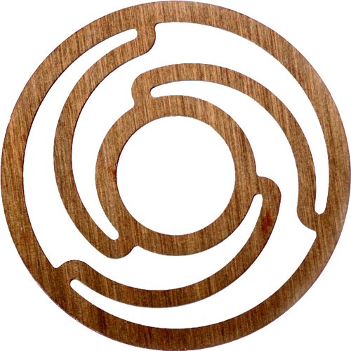
Photochemical Etching for the Photonics Industry
From emerging optical sensors to high-energy laser platforms, photonics drives innovation across a wide range of applications. In these environments, the difference between breakthrough performance and optical signal degradation often comes down to micro-scale metal features and alignment components that must be perfectly consistent.
As a core fabrication partner for companies pushing the boundaries of optics and photonics, Fotofab specializes in manufacturing extremely precise, flat, repeatable metal components essential to mission-critical photonic devices. Experts in the photochemical etching process, we support optical engineers, R&D teams, and production manufacturers with micro-apertures, precision masks, filters, light shields, flexures, reticles, encoder disks, and thin-metal structures down to ultra-fine geometries as small as 0.004″.
Why the Photochemical Etching Process is Ideal for Photonics
The unique demands of photonic systems make chemical etching the preferred process for many optical component geometries. Unlike laser cutting or stamping, photo etching produces features without mechanical force or heat input, eliminating stress, warping, and deformation.
With unmatched precision and flexibility, the photochemical machining process enables optical engineers to manufacture shapes and features that cannot be achieved with traditional machining methods at volume.
Key Advantages of Chemical Etching
Tight Tolerances on Thin Metals
Achieve dimensional accuracy required for beam definition, sensor alignment, and optical repeatability.
Burr-Free Edges—No Secondary Deburring Required
Burrs scatter light and compromise system performance. Photo etching ensures perfectly clean edges without the need for follow-up processing, even on intricate shapes.
Stress-Free, Flat Components
Because the etching process is chemical rather than mechanical, parts remain flat and free of any induced stress, protecting delicate optical assemblies.
Rapid Prototyping for R&D Cycles
Without hard tooling or long setups, prototypes can be produced quickly and iterated rapidly and easily.
Repeatable Accuracy for Scaled Production
Once a design is qualified, the etching process guarantees consistency across batches, from prototypes to volume production.
Low-Cost Tooling for Multi-Iteration Designs
Digital tooling enables affordable design changes, accelerating development cycles while reducing total manufacturing cost.Complex Ultra-Fine Geometries Down to 0.004″
Ideal for micro-apertures, filters, encoder disks, miniature springs, intricate grids, and precision optical features tied to beam shape and system performance.
For apertures, single sided etchings can even create precise funnels to focus optical signals further.
Photonics Applications Fotofab Supports
Medical Photonics
- Endoscopy and minimally invasive imaging systems
- Surgical laser assemblies
- Diagnostic optical platforms
- Micro-apertures, filters, masks, and alignment frames used in illumination and detection paths
Defense & Aerospace Photonics
- LIDAR optics and scanning assemblies
- Targeting and positioning sensors
- IR and thermal imaging systems
- Beam-shaping apertures
- EMI/RFI shielding components for photonic modules
Semiconductor & Technology
- Optical encoders and sensing wheels
- Photomasks and micro-patterning components
- Fiber-optic connectors and ferrule components
- Laser diode mounts and thermal management parts
- Micro-filters, grids, and shielding structures
- Heat sinks
- Microfluidic cooling
Telecom & Communications
- High-frequency optical pathway structures
- Precision spacers and shims for fiber alignment
- Fiber-optic switching and routing components
- View all markets
Parts Fotofab Fabricates for the Photonics Industry
Fotofab produces a wide range of precision thin-metal parts that enhance optical accuracy, mechanical stability, and thermal performance inside photonic systems.
- Optical apertures & micro-apertures
- Light shields, masks & filters
- Reticles
- Grids & meshes
- Encoder disks
- Alignment shims & spacers
- Beam-shaping plates
- Lead frames
- Flexure components
- Miniature springs
- Thermal control components
- Connector components
Diffusion bonding is also available for hermetic optical assemblies, protected sensor housings, sealed laser diode packages, and thermal-control components supporting high-power lasers.
Commonly Used Materials
The team at Fotofab etches a wide range of materials and can advise on thickness, performance, and application-specific requirements.
Fotofab works with a wide range of materials, including:
- Stainless steels (302, 304, 316, 17-7, and others)
- Copper alloys (copper, beryllium copper, brass, bronze)
- Nickel and nickel-silver
- Titanium
- Molybdenum
- Invar and Kovar for low-expansion optical components
Whether you’re designing an aperture, light shield, or alignment frame, our team can help match the right metal, sheet format, and material thickness to your application.
End-to-End Manufacturing for Optical Precision
Our capabilities extend far beyond the etching process, supporting photonic components from early concept through production.
- Rapid prototyping and fast turnaround times
- Plating and post-processing options
- Forming & stamping
- Heat treating
- Laser welding and spot welding support
- Assembly support
- Comprehensive inspection and quality assurance for micro-features
- Black oxide
- Black anodize
- Electropolising (e-polishing)
We can also combine etching with diffusion bonding to create hermetically sealed or thermally optimized components such as cooling of advanced laser and sensor systems.
Committed to Quality
Fotofab maintains strict quality controls to meet the demands of advanced photonics, supporting customers where optical performance is non-negotiable.
- ISO 9001:2015 certified
- ITAR Registered
- REACH & RoHS compliant
- Full material traceability
- Rigorous inspection protocols for high-precision optical components
Every part is manufactured with the consistency, documentation, and reliability required for mission-critical optical and photonic systems.

Fotofab is committed to quality.
A Precision Etching Process: Why Companies Choose to Partner with Fotofab
Photonics innovators trust Fotofab because we consistently deliver high-accuracy, repeatable parts that directly impact optical performance. With deep experience in advanced imaging, sensing, and laser technologies, we’ve built a reputation for reliability in mission-critical optical assemblies.
Clients rely on us for everything from fast R&D iterations to full-scale production, and for our ability to quickly produce, refine, and validate ultra-complex geometries. Backed by decades of thin-metal manufacturing expertise, we help bring next-generation optical systems to life.
Whether you’re developing a micro-aperture, thermal component, encoder disk, or optical shield, Fotofab ensures your optical components perform exactly as designed—every time.
