Chemical Etching Copper
Fotofab is a leader in the precision chemical etching of copper, offering components across a diverse range of industries. Our expertise extends from the etching of delicate copper foils for printed circuit boards to the creation of robust, corrosion-resistant parts suitable for harsh environments.
Benefit from a process that ensures exceptional electrical and thermal conductivity, essential for high-performance applications.
Contact us to explore how our copper etching solutions can elevate the efficiency and quality of your projects. Request a quote today to start transforming your designs into precision components.
Copper Chemical Etching
The most common industrial application of etched Copper services is the foil in printed circuit boards (PCBs); however, acid etching of Copper has limitless applications. Its properties can be enhanced for specific applications by creating an alloy with another metal. For example, adding Beryllium increases physical strength.
The Copper Etching Process
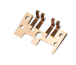
Copper chemical etching is an excellent process for applications in the electrical and electronic industries. This soft metal possesses high thermal and electrical conductivity and is one of the easier metals to photo-chemically machine or etch.
Fotofab’s chemical etching process produces designs with high corrosion resistance, capable of withstanding harsh indoor and outdoor environments. The process uses a copper etching solution, usually a strong caustic chemical like ferric chloride, to acid etch copper, creating a design or image formed to your project’s specifications.
Characteristics of Copper
Copper Alloys We Work With
- High electrical and thermal conductivity that is second only to Silver
- Durable for forming, stamping, bending, and chemical etching
- Corrosion-resistant which can be enhanced with plating or coating (important in high-frequency applications where “skin-effect” issues must be considered)
- Soft, ductile, and malleable so it can be drawn, “stretched,” or flattened in various shapes and sizes
- Accepts soldering without special preparation or materials
Fotofab is committed to quality.

Applications of Etched Copper
Copper is used in almost anywhere that there is an electrical circuit path on a printed circuit board, within an electrical component, such as a connector, or as a transitional device between circuit boards, including:
- Electrical contacts, pins, terminals, and connectors
- Formed metal enclosures for hybrid electronic circuits
- EMI/RFI shielding on printed circuit boards
- UHF/microwave antennas and waveguides
- Lead frames
- Inserts for injection molding
- Fuse links and bus bars
- Board-level EMI/RFI shields
- Shielded enclosures with snap-on lids
Other Factors
Copper is an abundant metal, but prices have historically varied with significant market fluctuations
It’s worth noting that bare copper can trigger electrochemical reactions when it comes into contact with certain metals. In applications where enhanced hardness is essential, a copper alloy such as brass, bronze, beryllium copper, or nickel silver is preferred. Each offers tailored properties to meet specific manufacturing requirements.
Copper-Molybdenum Etching
Copper-Molybdenum is a composite material that has similar thermal properties to Tungsten-Copper. Its low density makes it suitable for applications where weight limitations are a factor. The combination of high thermal conductivity and low thermal expansion makes Copper-Molybdenum perfect for semiconductor substrates, high-power devices, electrical contacts, and more.
Leveraging Copper with Fotofab
Our dedication to producing the highest quality precision metal components through chemical etching is reinforced by our certifications (ISO & AS9100D, ITAR Registration, RoHS compliance). Fotofab stands ready, whether for rapid prototyping or full-scale production of copper components.
Contact Our Precision Etching Experts today to discuss how we can integrate Fotofab’s advanced copper etching capabilities into your next metal component project.
