Precision Etching – Metal Etching Services at Fotofab
Burr-Free Precision Metal Components for Complex Engineering Applications
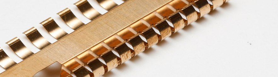
Fotofab provides precision chemical etching services that enable engineers to manufacture highly detailed metal components with exceptional accuracy, repeatability, and burr-free edge quality. Using advanced photochemical machining, we produce intricate geometries, fine apertures, precision meshes, and thin metal parts that are difficult to achieve with conventional manufacturing methods.
Unlike machining, stamping, or laser cutting, the photo etching process removes exposed metal chemically rather than mechanically, preserving material properties while eliminating burrs, heat-affected zones, and mechanical stress.
From rapid prototypes to full-scale production, Fotofab supports aerospace, defense, medical, semiconductor, electronics, and industrial customers with precision etching solutions tailored to demanding applications. Backed by decades of expertise, AS9100D and ISO 9001:2015 certifications, and extensive material capabilities, we help engineers confidently produce high-precision components.
What Is Precision Chemical Etching?
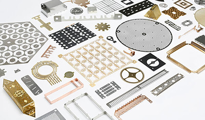
Precision chemical etching is a controlled subtractive manufacturing process that removes material from a metal sheet to produce intricate, dimensionally accurate components. Also known as photochemical machining or photo etching, it uses digital imaging and carefully controlled chemical solutions instead of cutting tools or heat.
A photoresist protects selected areas while a chemical etchant removes only the exposed metal, creating highly accurate features with clean, burr-free edges and excellent repeatability.
Because the process introduces no mechanical stress or heat-affected zones, it is ideal for manufacturing thin metal components with fine features, complex geometries, and consistent dimensional accuracy across a wide range of modern engineering applications.
Learn more: Download our Photochemical Machining (PCM) Whitepaper
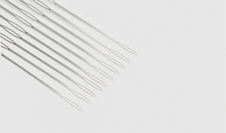
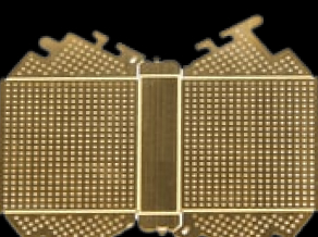
The Chemical Etching Process
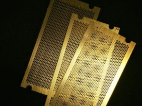
Every precision etched component begins with a CAD design and follows a tightly controlled manufacturing process. Unlike mechanical cutting methods, the photochemical machining process removes material using carefully controlled chemistry to produce intricate features with exceptional consistency.
Step 1: Digital Artwork and Photoresist Imaging
CAD data is converted into high-resolution phototools, and a light-sensitive photoresist is applied to both sides of the metal sheet. Ultraviolet light transfers the component pattern onto the resist, defining every feature of the finished part.
Step 2: Developing the Image
The unprotected photoresist is removed to expose selected areas of the metal while protecting the remaining surface. Because the artwork is digital, designs can be updated quickly without expensive hard tooling, making the process ideal for rapid prototyping and low-volume production.
Step 3: Controlled Chemical Etching
The sheet passes through an automated etching system where a chemical etchant, commonly ferric chloride for stainless steels and many copper alloys, removes only the exposed metal. Carefully controlled process parameters ensure burr-free features, excellent edge quality, and consistent dimensional accuracy.
Step 4: Inspection and Finishing
After etching, the photoresist is removed, and each component is inspected for dimensional accuracy and surface quality. Depending on the application, parts may then undergo secondary operations such as forming, plating, diffusion bonding, heat treating, or assembly.
Why Engineers Choose Precision Etching
Precision chemical etching is a preferred manufacturing process for producing increasingly complex components used in modern electronic devices, medical systems, aerospace assemblies, and semiconductor equipment. It enables features that are difficult or impossible to achieve with conventional fabrication methods.
Engineers choose precision etching when they need:
- Tight tolerances in thin materials
- Burr-free edges
- Fine apertures and complex geometries
- Stress-free manufacturing
- No heat-affected zones
- Rapid design iterations without expensive tooling
- Repeatable production from prototype to volume manufacturing
Because there is no direct tool contact, the process preserves material properties, grain structure, and flatness. This makes it ideal for manufacturing springs, flexures, diaphragms, EMI shielding, encoder discs, filters, precision shims, and other high-performance components where material integrity is as important as dimensional accuracy.
Precision Etching Capabilities
Engineers need confidence that their manufacturing partner can achieve tight tolerances, produce intricate geometries, support a range of materials, and scale from prototype to production. Fotofab combines disciplined process control with decades of photochemical machining expertise to deliver high-precision components with exceptional consistency.
Tolerance Capabilities
Precision chemical etching provides excellent dimensional accuracy, particularly in thin materials. Achievable tolerances depend on factors such as material type, metal thickness, feature geometry, and part size, with a general guideline of ±20% of material thickness.
Because there is no cutting tool to wear, the photo etching process delivers consistent dimensional accuracy and repeatable results throughout production.
Fine Feature Resolution
Precision etching excels at producing intricate features that are difficult to achieve with conventional manufacturing methods, including:
- Fine apertures
- Narrow slots
- Small holes
- Precision meshes
- High-density feature layouts
Because material is removed chemically rather than mechanically, closely spaced features can be produced without distortion, making the process ideal for delicate and highly detailed components.
Repeatability Across Production Runs
Strict control of photoresist imaging, chemistry, temperature, spray pressure, and inspection ensures consistent quality from prototype through high-volume production. This repeatability is essential for regulated industries where dimensional accuracy and reliable component performance are critical.
Complex Geometry Capability
Precision chemical etching enables engineers to manufacture intricate components that are difficult or costly to produce using conventional machining or stamping. By working directly from digital artwork, Fotofab produces parts with:
- Intricate internal profiles
- Fine slots and precision apertures
- Narrow webs
- Complex lattice structures
- High-density feature layouts
Because there is no physical cutting tool, increasing part complexity has minimal impact on manufacturing efficiency. This makes chemical etching metal an ideal solution for aerospace assemblies, RF shielding, optical components, sensors, precision filters, and modern electronic devices.
Thin Metal Components
Precision chemical etching is particularly effective for thin-gauge materials, where mechanical processes can cause warping, distortion, or edge damage.
The non-contact process preserves flatness and material properties, making it ideal for:
- Precision shims
- Springs and flexures
- Encoder discs
- Thin diaphragms
- EMI shields
- Screens and fine meshes
- Precision gaskets
As metal thickness decreases, the advantages of chemical etching become even greater than those of laser cutting, punching, and machining.
Prototype Through Production
The photochemical machining process supports every stage of product development, from rapid prototyping to full-scale production.
Rapid Prototyping
With no expensive hard tooling required, engineers can quickly update digital artwork and evaluate multiple design iterations. This accelerates product development while reducing cost and lead times.
Low-Volume Production
Precision chemical etching is a cost-effective solution for prototypes, engineering validation, pilot builds, and low-volume production, delivering production-quality components without the tooling costs of stamping or punching.
High-Volume Manufacturing
Once a design is validated, the same manufacturing process scales seamlessly to full production. Using the original digital artwork, Fotofab maintains the dimensional accuracy, repeatability, and quality established during development, reducing manufacturing risk.
Precision Etching Compared with Other Manufacturing Processes
Choosing the right manufacturing process involves balancing feature complexity, material selection, production volume, cost, lead time, and performance requirements.
For thin metal components with intricate geometries, precision chemical etching often offers significant advantages over other manufacturing processes, delivering burr-free edges, excellent repeatability, and low tooling costs.
| Requirement | Precision Chemical Etching | Laser Cutting | CNC Machining | Stamping |
| Burr-free edges | ✓ | Limited | Often requires deburring | Often requires deburring |
| No heat-affected zone | ✓ | ✕ | ✓ | ✓ |
| No mechanical stress | ✓ | ✓ | ✕ | ✕ |
| Fine feature capability | Excellent | Good | Moderate | Limited |
| Complex geometries | Excellent | Good | Moderate | Limited |
| Rapid design revisions | Excellent | Excellent | Moderate | Poor |
| Low tooling costs | ✓ | ✓ | ✓ | ✕ |
| High-density feature layouts | Excellent | Moderate | Moderate | Poor |
For engineers developing thin, highly detailed components, precision chemical etching frequently delivers the best combination of design freedom, dimensional accuracy, production flexibility, and cost efficiency.
Learn more: Download our Photochemical Machining (PCM) Whitepaper
Benefits of Precision Chemical Etching
Precision chemical etching enables engineers to produce high-precision components with intricate geometries while preserving material integrity. By removing material chemically rather than mechanically, the process delivers the accuracy, flexibility, and repeatability required across modern manufacturing.
Burr-Free Metal Parts
Because material is dissolved rather than cut, the chemical etching metal process produces naturally clean, burr-free edges with little or no secondary finishing. This improves assembly efficiency and is particularly valuable for medical devices, electronics, optical systems, aerospace assemblies, and semiconductor equipment.
No Heat-Affected Zones
Unlike laser cutting, the photo etching process introduces no thermal energy, eliminating heat-affected zones, distortion, and residual stresses. Material properties remain unchanged, making precision etching ideal for aerospace, medical, defense, and electronics applications.
Stress-Free Manufacturing
The photochemical machining process is completely non-contact, applying no mechanical force to the workpiece. Components remain flat while preserving their grain structure and mechanical properties, making the process ideal for springs, flexures, precision shims, encoder discs, diaphragms, sensor components, and precision screens.
Exceptional Feature Accuracy
Precision etching produces fine apertures, small slots, intricate meshes, dense feature layouts, and other complex patterns with outstanding consistency. Because features are defined by digital artwork rather than cutting tools, increasing complexity has minimal impact on manufacturing efficiency.
Rapid Iteration Without Tooling
Using digital phototools instead of hard tooling allows engineers to update designs quickly and cost-effectively. This accelerates product development, supports rapid prototyping, and makes precision etching an excellent choice for research, development, and low-volume production.
Production Repeatability
Strict control of photoresist imaging, ferric chloride concentration, chemical solutions, temperature, spray pressure, and inspection ensures predictable, repeatable production from prototype through full-scale manufacturing.
Cost-Effective for Complex Parts
Unlike machining or wire EDM, complex geometries do not significantly increase manufacturing costs. Precision etching efficiently produces high-density feature layouts, fine apertures, thin metal components, intricate filters, and lightweight structures while keeping tooling costs low.
Material Versatility
Fotofab supports precision etching across a wide range of engineering materials, including stainless steels, titanium, aluminum, copper and copper alloys, brass, Kovar, Inconel, molybdenum, Nitinol, beryllium copper, phosphor bronze, and Mu Metal. Our engineers help customers select the best material based on performance, material compatibility, and manufacturability.
Supporting Modern Manufacturing
As products become smaller and more complex, precision chemical etching enables smaller feature sizes, greater design freedom, faster development, and consistent production. From modern electronic devices and medical instrumentation to heat exchangers, RF shielding, aerospace assemblies, and semiconductor equipment, precision etching continues to expand what’s possible in precision metal manufacturing.
Materials for Precision Etching
Selecting the right material is just as important as choosing the right manufacturing process. Mechanical strength, corrosion resistance, electrical conductivity, thermal performance, and manufacturability all influence component performance and long-term reliability.
Fotofab supports precision chemical etching across a broad range of engineering metals, helping engineers select the best material for their application while optimising manufacturability and cost.
Whether you’re designing aerospace components, medical devices, semiconductor equipment, or EMI shielding for modern electronic devices, our engineering team can recommend the most suitable material for your project.
Explore our Materials Hub to compare engineering materials and identify the best option for your application, or visit our individual material pages for detailed guidance on etchability, properties, and typical applications.
Fotofab is committed to quality.



Metal Etching Experts
The Fotofab precision etching process features a trio of fundamental improvements over other manufacturers, including reduced costs, faster speeds, and higher precision parts. We also source materials and manufacture completely within the United States.
We specialize in:
Metals We Chemically Etch
Fotofab provides precision chemical etching across a wide range of metals:
| Metal Name | Description | Available Alloys |
| Stainless Steel | Stainless Steel, an iron-based alloy enriched with Chromium and Nickel, is known for its exceptional physical strength and resistance to corrosion. | 301, 304, 316, 17-7 PH |
| Steel | Steel is a ferrous alloy metal, composed primarily of Iron, Carbon and other elements added depending on the characteristics desired. Steel is highly durable with a hardness that resists external strain over time. | 1008, 1010, 1075, 1095 |
| Titanium | Titanium is a corrosion-resistant metal with strong and lightweight properties. | Grade 2, Grade 5 |
| Nickel | Nickel is a silvery-white lustrous metal with a slight golden tinge. It belongs to the transition metals and is one of only four elements that are magnetic near or room temperature. | 200, 201 |
| Nickel Silver | Nickel Silver is an electronic-grade alloy with high thermal and electrical conductivity characteristics. Despite the alloy’s name and shiny appearance, it contains no Silver. | C71500, C77000 |
| Phosphor Bronze | Phosphorus Bronze is a tough alloy characterized by high strength, low coefficient of friction, and fine grain structure. | C51000, C52100 |
| Kovar | Kovar is a Nickel-Cobalt ferrous alloy invented to meet the need for a reliable glass-to-metal seal required in electronic devices. | F15 |
| Invar | Invar is a Nickel-Iron alloy notable for its low coefficient of thermal expansion. Like other Nickel/Iron compositions, Invar is a single-phase alloy, consisting of around 36% Nickel and 64% Iron. | 36 |
| Aluminum | Aluminum is a lightweight, highly conductive, reflective, and non-toxic metal. Its durability and corrosion-resistant properties make Aluminum chemical etching ideal for components in a variety of industries. | 1100, 2024, 3003, 5052, 6061 |
| Beryllium Copper | Beryllium Copper (BeCu) is a pliable metal alloy with high electrical conductivity. Beryllium Copper chemical etching is ideal for applications in electrical and electronic industries, such as contact and spring contact applications. | C17200, C19000 |
| Brass | Brass is a binary alloy composed of Copper and Zinc. It is similar to Bronze and valued for its workability, hardness, corrosion resistance, and attractive appearance. | C26000 |
| Copper | Copper chemical etching is an excellent process for applications in the electrical and electronic industries. This soft metal possesses high thermal and electrical conductivity and is one of the easier metals to photo-chemically machine or etch. | C11000, C10100, C26000, C51000, C52100, C71500, C77000 |
Explore All The Metals We Chemically Etch
Design Considerations for Precision Etching
Successful precision chemical etching starts with good design. While the photochemical machining process offers exceptional design freedom, factors such as feature size, metal thickness, tolerances, and part geometry all influence manufacturability and final part quality.
Fotofab works closely with engineers during Design for Manufacturability (DFM) reviews to optimize designs before production, helping reduce development time, improve yields, and minimize costly revisions.
Feature Size and Resolution
One of the key advantages of precision etching is its ability to produce fine features with exceptional consistency. Using high-resolution photoresist imaging instead of cutting tools, the photo etching process can create:
- Fine apertures
- Narrow slots
- Small holes
- Precision meshes
- High-density feature layouts
- Complex internal profiles
Because there is no physical cutting tool, intricate features can be reproduced accurately across the entire metal sheet without introducing distortion or increasing manufacturing complexity.
Metal Thickness and Etch Factor
Metal thickness directly affects achievable feature size, tolerances, and part geometry. Thinner materials allow finer features and tighter dimensional control, while thicker materials may require design adjustments to maintain manufacturability.
Another important consideration is the etch factor. During the etching process, material is removed both vertically and laterally, creating a predictable amount of undercut. Fotofab compensates for this during artwork preparation to achieve the required finished dimensions and maintain tight tolerances.
Dimensional Tolerances
Tolerance capability depends on material type, thickness, feature geometry, and overall part size. As a general guideline, achievable tolerances are approximately ±20% of material thickness, although tighter tolerances may be possible depending on the application.
During DFM reviews, our engineers identify critical dimensions and recommend practical tolerance strategies that balance performance, manufacturability, and cost.
Part Geometry and Flatness
Precision chemical etching supports highly complex geometries that would be difficult or costly to manufacture using conventional machining or stamping. When designing components, engineers should consider factors such as hole-to-edge spacing, minimum bridge widths, slot aspect ratios, and panel layout to maximise manufacturing efficiency.
Because the process introduces no heat or mechanical stress, components remain exceptionally flat with clean, burr-free edges. This makes precision etching ideal for aerospace, semiconductor, optical, and electronic applications where dimensional stability is critical.
Panelisation for Efficient Production
Multiple components can be nested within a single metal sheet, improving material utilisation, increasing throughput, and reducing manufacturing costs. During layout optimisation, Fotofab balances production efficiency with inspection accessibility and dimensional accuracy to maximise overall yield.
Engineering Support from Concept to Production
The most successful projects begin with early engineering collaboration. Fotofab’s Design for Manufacturability (DFM) process helps optimize:
- Material selection
- Feature resolution
- Tolerance requirements
- Etch factor compensation
- Panel layout
- Secondary operations
- Prototype development
- Production planning
Whether you’re comparing manufacturing processes, reviewing CAD files, or preparing a design for production, our engineering team provides practical guidance to ensure your component fully leverages the capabilities of precision chemical etching while reducing development risk and accelerating time to market.
Applications for Precision Chemical Etching
Precision chemical etching supports industries where burr-free edges, tight tolerances, and repeatable manufacturing are essential. By producing complex geometries without introducing heat or mechanical stress, the photo-etching process enables high-precision components that are difficult or costly to manufacture using other manufacturing processes.
From rapid prototypes to full-scale production, Fotofab supports customers across aerospace, defense, medical, semiconductor, electronics, and industrial markets.
Aerospace & Defense
Precision chemical etching produces lightweight, high-performance components for demanding aerospace and defense applications where dimensional accuracy and material integrity are critical.
Typical applications include:
- Precision shims
- RF and microwave components
- EMI shielding
- Sensor components
- Optical encoder discs
- Precision filters
- Aerospace brackets
- Precision mechanical assemblies
With no heat-affected zones or mechanical deformation, precision etching is ideal for thin components used in aircraft, satellites, avionics, radar systems, and other advanced defense technologies. Fotofab’s AS9100D-certified quality system supports the stringent requirements of these industries.
Medical Devices
The medical device industry relies on precision etching to manufacture intricate components with burr-free edges, smooth finishes, and consistent dimensional accuracy.
Common applications include:
- Surgical instruments
- Implant components
- Catheter components
- Medical sensors
- Diagnostic equipment
- Precision medical screens
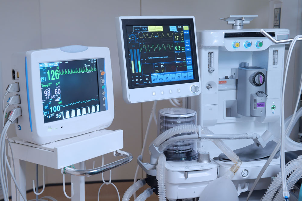
The process preserves the properties of specialized materials such as titanium and Nitinol, making it well suited to high-performance medical applications.
See how we service the Medical Device and Medical Implantable sectors.
Semiconductor Equipment
Semiconductor manufacturing requires extremely precise components capable of performing in cleanroom and vacuum environments.
Precision etching is used to manufacture:
- Precision apertures
- Wafer handling components
- Vacuum system parts
- Process equipment components
- Alignment features
- Fine meshes
Its ability to produce intricate features with exceptional repeatability makes it ideal for next-generation semiconductor equipment.
See how we service the Semiconductor industry.
Electronics & RF Systems
As modern electronic devices become smaller and more sophisticated, precision etching enables the production of highly detailed conductive components with excellent dimensional consistency.
Applications include:
- EMI/RFI shielding
- RF shielding
- Electrical contacts
- Connectors
- Lead frames
- Antenna components
- Sensor housings
Copper and copper alloys are commonly used for their excellent electrical conductivity and compatibility with precision etching.
See how we service the Electronics sector.
Industrial Equipment
Precision chemical etching supports a wide range of industrial applications requiring durable, repeatable, and cost-effective metal components.
Common applications include:
- Precision filters
- Fine screens
- Heat exchangers
- Flow control devices
- Precision gaskets
- Mechanical spacers
- Process equipment
Low tooling costs and the ability to manufacture complex geometries make precision etching an economical solution for both prototype and production applications.
See how we service the Industrial sector.
Supporting Diverse Engineering Applications
Whether you’re developing aerospace assemblies, medical devices, semiconductor equipment, RF shielding, industrial filters, or precision sensor components, Fotofab delivers the precision, repeatability, and engineering expertise needed to support demanding applications.
With broad material capabilities, decades of manufacturing experience, and scalable production from prototype through volume manufacturing, we help engineers bring complex metal components to life with confidence.
Why Choose Fotofab for Chemical Etching Services
The expert team at Fotofab brings decades of experience and expertise in photo chemical machining and precision metal fabrication. Our U.S.-based manufacturing operations are built around process control, engineering collaboration, and repeatability.
We focus exclusively on high-precision etching solutions, enabling us to refine our methods continuously and deliver consistent results.
The Fotofab difference:
Quality and Repeatability
Process control and inspection systems ensure that each batch meets specification—whether prototype or production.
Engineering-First Approach
We prioritize early-stage technical collaboration, ensuring optimal outcomes before manufacturing begins.
Proven Across Industries
Our precision chemical etching services support demanding industries requiring consistent, high-quality custom metal parts.
A Certified Manufacturing Team You Can Trust
As a preferred supplier of custom-made precision metal parts to hundreds of leaders in the aerospace, defense, medical, telecommunications, and electronics industries, Fotofab is committed to quality, which is shown through our various certifications.
Fotofab is proud to have earned both AS9100D and ISO 9001:2015 certifications. The quality standards covered by this certificate include ISO 9001, DoD, NASA, and FAA requirements. Fotofab is also a proudly ITAR-registered manufacturer.
Learn more: Download our Photochemical Machining (PCM) Whitepaper
Frequently Asked Questions
What is the difference between photochemical etching and acid etching?
Photochemical etching uses photoresist imaging and controlled chemical etchants, such as ferric chloride, to selectively remove exposed metal. While it’s sometimes called acid etching, modern photochemical etching offers far greater accuracy, repeatability, and process control, making it ideal for manufacturing intricate metal components with tight tolerances, burr-free edges, and complex geometries.
What industries use photochemical etching?
Photochemical etching is used across industries requiring high-precision components, including aerospace and defense, medical devices, electronics, semiconductor manufacturing, telecommunications, and industrial equipment.
Typical applications include aerospace fuel cell components, printed circuit boards (PCBs), microelectromechanical systems (MEMS), surgical instruments, stents, EMI shielding, and precision sensors, where dimensional accuracy and repeatability are essential.
Can photochemical etching be used to manufacture medical devices?
Yes. Photochemical etching is widely used in the medical device industry to manufacture surgical instruments, stents, catheter components, implantable devices, and diagnostic equipment. Because the process introduces no heat or mechanical stress, it preserves material properties while producing the fine features, burr-free edges, and tight tolerances required for precision medical applications.
What are the limitations of chemical etching?
Like any manufacturing process, precision chemical etching has design considerations. Controlling the etching rate can become more challenging with highly complex geometries, and variations in substrate material may influence etching consistency if process parameters are not carefully managed. The process also generates liquid waste that must be handled and treated responsibly in accordance with environmental regulations.
These challenges are addressed through disciplined process control, Design for Manufacturability (DFM) reviews, and rigorous quality systems. At Fotofab, careful control of chemistry, material selection, and production parameters helps ensure consistent, repeatable results while minimising process variation and environmental impact.
Is photochemical etching suitable for electronics manufacturing?
Yes. Photochemical etching is widely used to manufacture precision components for printed circuit boards (PCBs), microelectromechanical systems (MEMS), EMI/RFI shielding, electrical contacts, connectors, lead frames, RF components, and sensor elements. Its ability to produce intricate patterns with excellent dimensional accuracy makes it ideal for today’s compact, high-performance electronic devices.
Why is chemical etching used for aerospace fuel cell components?
Fuel cell components often require fine flow paths, precision apertures, and complex geometries that are difficult to manufacture using conventional methods. Chemical etching produces these intricate features without introducing heat-affected zones or mechanical stress, making it well suited to aerospace fuel cell systems and other high-performance applications requiring exceptional precision and repeatability.
Work with one of the Leading Chemical Etching Companies
If you are evaluating chemical etching companies for your next project, Fotofab stands ready to support you. We encourage early-stage design discussions and engineering reviews to ensure your part is optimized for the chemical etching process.
Contact our precision etching experts today to discuss how Fotofab’s advanced precision etching capabilities can support your next generation of precision metal components.