This website uses cookies so that we can provide you with the best user experience possible. Cookie information is stored in your browser and performs functions such as recognising you when you return to our website and helping our team to understand which sections of the website you find most interesting and useful.
Fotofab History
You the customer are the reason why Fotofab has achieved success over the past 55 years. Fotofab is committed to your satisfaction
Our mission is to deliver precision metal components to industry leaders with expertise, reliability, and quality.
Our Etching History
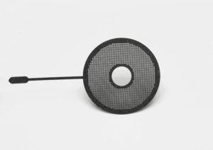
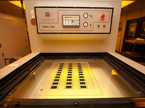
Etching has been around since the Middle Ages. It was used during that time to decorate armor. By the 16th century, it was used by printmakers to produce printing plates.
The process was developed as a manufacturing process by The Buckbee Mears Corporation from St. Paul, MN in the early 1900s and then further developed by Kodak during the 1960s. Kodak wanted to sell more film and photoresist so they ran a seminar on how to produce sheet metal parts via photo-etching.
The Fotofabrication Corporation was founded in 1967 in Chicago, IL as a result of those seminars. Buckbee Mears went on to produce shadow masks for a large percentage of the cathode ray TV sets manufactured in America and throughout the world.
Fun Facts
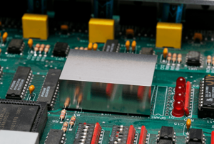
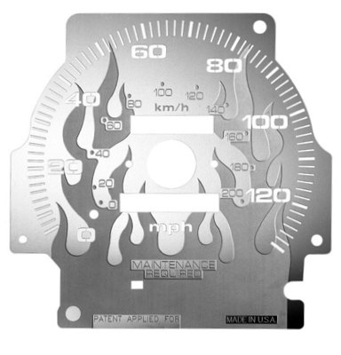
You have used a photo-etched product whether you know it or not, every electronic device made contains an electronic circuit board manufactured by chemical etching.
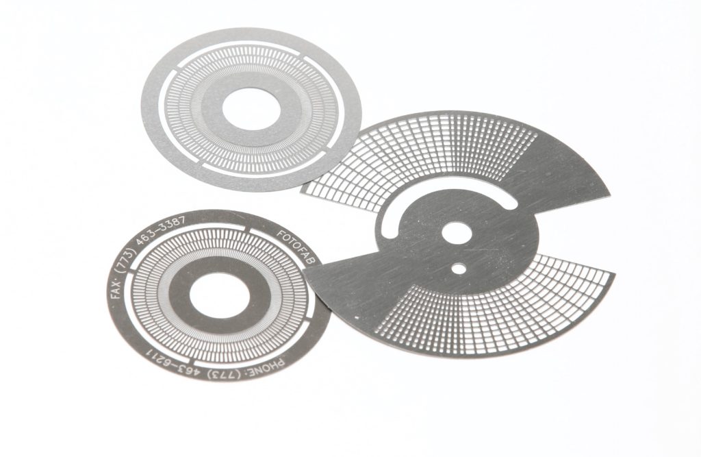
Fotofab provides a wide range of high-precision metal fabricating services to produce components with geometries from simple to very complex. Whether the mission is a quick-turn prototype or a high-volume production run, Fotofab has been satisfying engineers for five decades.
And while our core competency has not changed over that time, the technology of our production tools continues to evolve. As we look to the next decade, we see opportunities for our customers to benefit from our unrivaled experience, while knowing that their parts will be produced with state-of-the-art production methodologies and uncompromising quality standards.
Today, Fotofab is highly regarded by our customers for being responsive to their needs for product quality, quick response times, and highly knowledgeable customer service. Located on Chicago‘s Northwest Side, our main plant houses multiple etching machines and a thoroughly equipped CAE/CAD department. Our tooling, forming, and stamping facility is located in Elk Grove Village, a short drive from our main facility and very close to O’Hare airport.
Our Certifications
We are proud to have earned our AS9100D and ISO 9001 certifications, we are ITAR registered and are RoHS compliant. See more about our certifications on our Certifications Page.
Fotofab is committed to quality.


Our Commitment to the Environment
We are also seeing greater customer emphasis on environmental issues. Fotofab had anticipated this growing trend and is well-positioned to satisfy these customer concerns. We are particularly proud to have been commended by government regulatory agencies for our environmental compliance and cooperation.
Fotofab believes that to achieve long-term growth, we must be good stewards of the environment. We constantly work toward making our manufacturing process cleaner, safer, and even more respectful of our country’s natural resources.
Our Commitment to the Future of the Industry
Looking ahead to the next 10 years, Fotofab will continue to invest in the latest technologies to continue our commitment to continuous improvement. Advances in CAD systems will help engineers simplify design tasks and shorten the overall project cycles.
Gradual refinements on the manufacturing side will also help speed production while maintaining the company’s well-known tight tolerances.
Looking forward to our customers’ applications – the trend in the electronics industry is for smaller, lighter, and more efficient products with even tighter tolerances.
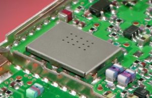
For example, in order to make power supplies smaller, they must operate at higher frequencies, creating a greater need for shielding and heat dissipation. Our processes can satisfy those needs without lengthening product development time.
Be it medical, aerospace, electronics, or any other market, customer companies will continue to push out new designs faster than ever. Fotofab takes pride in being able to stay a step ahead of our customers’ needs with affordable, quick-turnaround custom parts for prototypes. In addition, we are well-equipped in moving prototypes to laser production runs.
Another area of change is the types of metals our customers are asking us to fabricate. Exotic metals are required for some medical, aerospace, and scientific applications, because of their unique properties. These same properties can be challenging when the metal is etched, stamped, or formed.
Fotofab has developed proprietary approaches to overcoming these challenges so that we are able to deliver parts that are comparable to those made of more compliant metals.
In summary, Fotofab will continue to maintain close relationships with our customers and advance our capabilities to keep pace with their future needs. The longevity and professionalism of our staff ensure the highest level of satisfaction.
Short-Run and Full-Run Production for Your Market
A Partner Company
Fotofab is a proud member of The Partner Companies group of specialty manufacturers who share a commitment to excellence, precision, and innovation. TPC companies operate as a consortium of capabilities, serving the defense, aerospace, medical, telecommunications, semiconductor, and renewable energy industries.
TPC supports each member entity with expertise in business growth, finance, human resources, and supply chain management. The strength of TPC is the sharing of experience, materials, and resources that its members share.
Visit the TPC website

